1
Rev. 3/6/03
SP2954 250mA Low Dropout Voltage Regulator
© Copyright 2003 Sipex Corporation
250mA Low Dropout Voltage Regulator
SPX2954
DESCRIPTION
FEATURES
5.0V and 3.3V Versions at 250mA
Output
Accurate 0.5% for SPX2954A
Very Low Quiescent Current
Low Dropout: 310mV at 250mA
Extremely Tight Load and Line Regulation
Very Low Temperature Coefficient
Current and Thermal Limiting
Need only 1
µ
F for Stability
Direct Replacement for LP2954
Offered in TO-92, TO-263, SOT-223,
TO-220 and SOIC
8 Pin Versions Only
Error Flag Warns of Output Dropout
Logic-Controlled Electronic Shutdown
Programmable Output from 1.24V to 30V
Æ
The SPX2954 and SPX2954A are low power voltage regulators. These devices are an excellent
choice for use in battery-powered applications such as cordless telephones, radio control
systems, and portable computers. The SPX2954 and SPX2954A feature low quiescent current
and low dropout voltage (typ. 20mV at 100
µ
A and 310mV at 250mA). This includes a tight initial
tolerance (0.5% for SPX2954A), extremely good load and line regulation (0.05% typ.), and very
low output temperature coefficient (20 ppm/
∞
C typ.), making the SPX2954/SPX2954A useful as
a low-power voltage reference.
The error flag output feature is used as a power-on reset for warning of a low output voltage, due
to a falling input voltage. The logic-compatible shutdown feature enables the regulator to be
switched ON and OFF. The SPX2954/SPX2954A is offered in 3-pin TO-92, TO-263, SOT-223
and TO-220 packages, and 8 pin SOIC package.
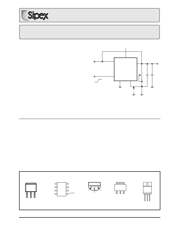
100K
OUTPUT
ERROR
ERROR
______
SD
V
OUT
GND
FB
+V
IN
+V
IN
1.23V
1.2 to 30V
R
1
.01
µ
F
3.3
µ
F
R
2
V
REF
3
8
5
1
4
7
SHUTDOWN
INPUT
+
SPX2954
Adjustable Regulator
Pin Connections
TO-263-5 Package (T5)
Top View
4 5
SPX2954
TO-263-3 Package (T)
GND
GND
SHUTDOWN
ERROR
1)
3)
4)
5)
2) OUTPUT
INPUT
SPX2954
Top View
1
2
3
3
2
1
V
OUT
V
IN
Top View
2
1
3
4
8
7
6
5
SPX2954
SHUTDOWN
GND
INPUT
5V, 3.3V TAP
ERROR
FEEDBACK
SENSE
OUTPUT
8-Pin Surface Mount (S)
Bottom View
1
3
2
OUTPUT
GND
INPUT
TO-92 (N)
SPX2954
1
3
2
V
OUT
GND
SOT-223 Package (M3)
Front View
V
IN
TO-220-5 Package (U5)
Front View
SPX2954
GND
SHUTDOWN
ERROR
1)
3)
4)
5)
2) OUTPUT
INPUT
1 2 3 4 5
Front View
TO-220-3 Package (U)
SPX2954
1
2
3
V
IN
V
OUT
GND

Rev. 3/6/03
SP2954 250mA Low Dropout Voltage Regulator
© Copyright 2003 Sipex Corporation
2
ABSOLUTE MAXIMUM RATINGS
Power Dissipation........................................Internally Limited
Lead Temperature (soldering, 5 seconds) ................260
∞
C
Storage Temperature Range........................-65
∞
C to +150
∞
C
Operating Junction Temperature Range......-40
∞
C to +125
∞
C
Input Supply Voltage...........................................-0.3V to +30V
Feedback Input Voltage....................................-1.5V to +30V
Shutdown Input Voltage .................................-0.3V to +30V
Error Comparator Output...................................-0.3V to +30V
ESD Rating................................................................2kV Min
SPX2954A
SPX2954
PARAMETER
CONDITIONS
MIN.
TYP.
MAX
MIN.
TYP. MAX.
UNIT
3.3 V Versions
Output Voltage
T
J
=25
∞
C
3.284
3.3
3.317
3.267
3.3
3.333
V
-25
∞
C
T
J
85
∞
C
3.267
3.3
3.333
3.251
3.3
3.350
Full Operating Temp.
3.260
3.3
3.340
3.234
3.3
3.366
Output Voltage
100
µ
A
I
L
250 mA
3.251
3.3
3.350
3.201
3.3
3.399
V
T
J
T
JMAX
5 V Versions
Output Voltage
T
J
= 25
∞
C
4.975
5.0
5.025
4.950
5.0
5.050
V
-25
∞
C
T
J
85
∞
C
4.950
5.0
5.050
4.925
5.0
5.075
Full Operating Temp.
4.940
5.0
5.060
4.900
5.0
5.100
Output Voltage
100
µ
A
I
L
250 mA
4.925
5.0
5.075
4.850
5.0
5.150
V
T
J
T
JMAX
All Voltage Options
Output Voltage
(N
OTE
1)
20
100
50
150
ppm/
∞
C
Temperature Coefficient
Line Regulation (N
OTE
3)
V
O
+1V
V
IN
30V |
0.03
0.10
0.04
0.20
%
(N
OTE
4)
Load Regulation (N
OTE
3)
100
µ
A
I
L
250 mA
0.04
0.20
0.10
0.30
%
Dropout Voltage
I
L
= 1mA
60
100
60
100
mV
(N
OTE
5)
I
L
= 100 mA
290
450
290
450
I
L
= 250 mA
310
500
310
500
Ground Current
I
L
= 1mA
150
170
150
170
µ
A
I
L
= 100 mA
3
6
3
6
mA
I
L
= 250 mA
10
14
10
14
mA
Current Limit
V
OUT
= 0
270
550
270
550
mA
Thermal Regulation
0.05
0.2
0.05
0.2
%/W
Output Noise,
C
L
= 1
µ
F
430
430
µ
V rms
10Hz to 100kHz
C
L
= 200
µ
F
160
160
µ
V rms
C
L
= 3.3
µ
F, Bypass=
100
100
µ
V rms
0.01
µ
F from Pin 7 to
Pin 1 (8 pin Versions)
8-Pin Versions only
Reference Voltage
1.220
1.235
1.250
1.210 1.235 1.260
V
Reference Voltage
Over Temp (N
OTE
6)
1.190
1.270
1.185
1.285
V
Feedback Pin
40
60
40
60
nA
Bias Current
Vref Temperature
20
50
ppm/
∞
C
Coefficient
Feedback I
BIAS
0.1
0.1
nA/
∞
C
Temperature Coefficient
ELECTRICAL CHARACTERISTICS
V
IN
=V
O
+ 1V, I
L
=100
µ
A, C
L
=1
µ
F (
NOTE
2), T
A
= 25
∞
C, unless otherwise specified.
3
Rev. 3/6/03
SP2954 250mA Low Dropout Voltage Regulator
© Copyright 2003 Sipex Corporation
ELECTRICAL CHARACTERISTICS (Cont.)
V
IN
=V
O
+1V, I
L
=100
µ
A, C
L
=1
µ
F (
NOTE
2), T
A
= 25
∞
C, unless otherwise specified.
N
OTE
1: Output or reference voltage temperature coefficients defined as the worst case voltage change divided
by the total temperature range.
N
OTE
2: Unless otherwise specified all limits guaranteed for T
J
= 25
∞
C, V
IN
= 6V, I
L
= 100
µ
A and C
L
= 1
µ
F.
Additional conditions for the 8-pin versions are feedback tied to 5V tap and output tied to output sense
(V
OUT
= 5V) and V
SHUTDOWN
0.8V.
N
OTE
3: Regulation is measured at constant junction temperature, using pulse testing with a low duty cycle.
Changes in output voltage due to heating effects are covered under the specification for thermal
regulation.
N
OTE
4: Line regulation for the SPX2954 is tested at I
L
= 1mA.
N
OTE
5: Dropout voltage is defined as the input to output differential at which the output voltage drops 100mV
below its nominal value measured at 1V differential. At very low values of programmed output voltage,
the minimum input supply voltage of 2V (2.3V over temperature) must be taken into account.
N
OTE
6: V
REF
V
OUT
(V
IN
- 1V), 2.3
V
IN
30V, 100
µ
A
I
L
250mA, T
J
T
JMAX
.
N
OTE
7: Comparator thresholds are expressed in terms of a voltage differential at the feedback terminal below
the nominal reference voltage measured at 6V input. To express these thresholds in terms of output
voltage change, multiply by the error amplifier gain = V
OUT
/V
REF
= (R
1
+ R
2
)/R
2
. For example, at a
programmed output voltage of 5V, the error output is guaranteed to go low when the output drops by 95
mV x 5V/1.235 = 384 mV. Thresholds remain constant as a percent of V
OUT
as V
OUT
is varied, with the
dropout warning occurring at typically 5% below nominal, 7.5% guaranteed.
N
OTE
8: V
SHUTDOWN
2V, V
IN
30V, V
OUT
=0, Feedback pin tied to 5V/3.3V Tap.
SPX2954A
SPX2954
PARAMETER
CONDITIONS
MIN.
TYP.
MAX
MIN.
TYP. MAX.
UNIT
Error Comparator
Output Leakage Current
V
OH
= 30V
0.01
1
0.01
1
µ
A
Output Low Voltage
V
IN
= V
O
-0.5V,
I
OL
= 400
µ
A
150
250
150
250
mV
Upper Threshold Voltage
(N
OTE
7)
40
60
40
60
mV
Lower Threshold Voltage
(N
OTE
7)
75
95
75
95
mV
Hysteresis
(N
OTE
7)
15
15
mV
Shutdown
Input logic Voltage
Low (Regulator ON)
1.3
0.7
1.3
0.7
V
High (Regulator OFF)
2.0
2.0
Shutdown Input Current
VS = 2.4V
30
50
30
50
µ
A
VS= 30V
400
800
400
800
Regulator Output Current
(N
OTE
8)
3
10
3
10
µ
A
in Shutdown
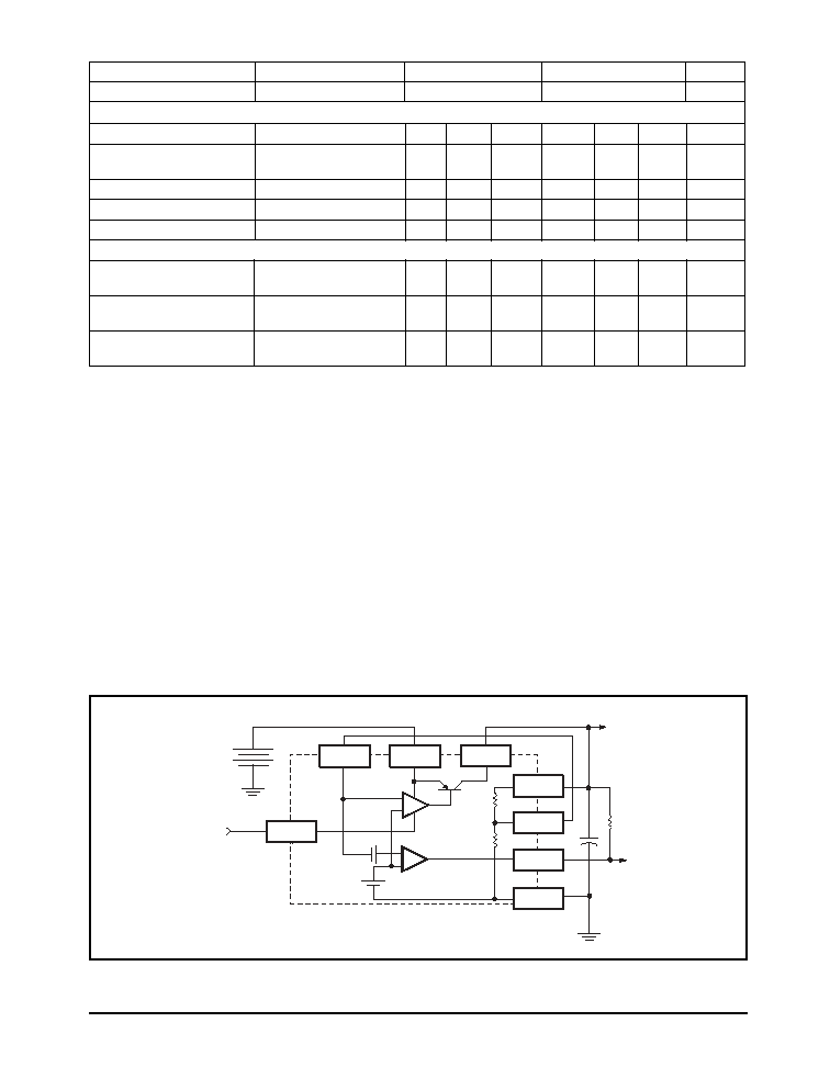
SPX2954 Block Diagram, 8 Lead 5V Version
INPUT
OUTPUT
UNREGULATED DC
SHUTDOWN
GROUND
ERROR
______
SENSE
TO CMOS OR
TTL
REFERENCE
ERROR DETECTION
COMPARATOR
ERROR
AMPLIFIER
1.23V
FROM
CMOS OR
TTL
+
+
+
+
+
+
60 mV
3
7
8
1
2
6
5
4
60k
330k
180k
.
.
1
µ
F
_
_
FEEDBACK
5V TAP
5V
Rev. 3/6/03
SP2954 250mA Low Dropout Voltage Regulator
© Copyright 2003 Sipex Corporation
4
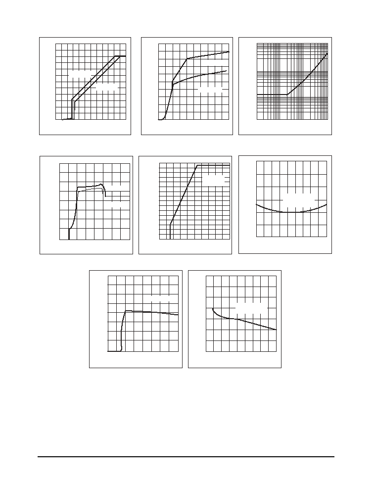
TYPICAL PERFORMANCE CHARACTERISTICS
Input Current
IN
PU
T
C
U
R
R
E
N
T
(
µ
A
)
75
0
0
10
INPUT VOLTAGE (VOLTS)
R
L
= 50k
25
50
100
125
150
175
200
225
250
1
2
3
R
L
=
8
Dropout Characteristics
O
U
T
PU
T
VO
LTA
G
E
(V
O
LT
S)
0
0
INPUT VOLTAGE (VOLTS)
1
2
3
4
5
6
1
2
3
4
5
6
R
L
=50k
R
L
=50k
4
5
6
7
8
9
LOAD CURRENT (mA)
Quiescent Current
G
RO
U
N
D
PIN
C
U
R
R
EN
T
(m
A
)
10
1
0.1
0.01
0.1
1
10
100
Ground Current
G
RO
U
N
D
C
U
R
R
E
N
T
(
µ
A
)
320
280
0
INPUT VOLTAGE (VOLTS)
240
80
40
0
1
2
3
4
5
6
7
8
120
160
200
I
L
= 1mA
I
L
= 0
INPUT VOLTAGE (VOLTS)
Input Current
IN
PU
T
C
U
R
R
E
N
T
(m
A
)
160
150
140
130
70
50
0
120
110
100
90
80
60
40
30
20
10
0
1
2
3
4
5
6
7
8
9 10
R
L
=50
V
OUT
= 5V
Quiescent Current
190
170
150
130
-75 -50 -25
0
25
50
75 100 125 150
TEMPERATURE (∫C)
Q
U
IESC
E
N
T
C
U
R
R
E
N
T
(
µ
A
)
V
IN
=6V
I
L
=100uA
Ground Current
8
7
6
0
1
2
3
4
5
6
7
8
INPUT VOLTAGE
G
RO
U
N
D
C
U
R
R
E
N
T
(m
A
)
5
4
3
2
1
0
I
L
=100mA
Ground Current
6
5
4
3
-75 -50 -25
0
25
50
75 100 125 150
TEMPERATURE (∫C)
G
RO
U
N
D
C
U
R
R
E
N
T
(m
A
)
V
IN
= 6V
I
L
= 100mA

5
Rev. 3/6/03
SP2954 250mA Low Dropout Voltage Regulator
© Copyright 2003 Sipex Corporation
TYPICAL PERFORMANCE CHARACTERISTICS
(CONT.)
Comparator Sink Current
SIN
K
C
U
R
R
E
N
T
(m
A
)
2.5
1.5
OUTPUT LOW VOLTAGE (V)
2.0
1.0
0.5
0.0
0.0 0.1 0.2 0.3 0.4 0.5 0.6 0.7 0.8
0.9
T
A
= -55∫C
T
A
= 25∫C
T
A
= 125∫C
Line Transient Response
TIME(
µs)
100
0
200
400
600
800
IN
P
U
T
O
U
T
P
U
T
VO
LTA
G
E
VO
LTA
G
E
C
H
A
N
G
E
4V
6V
8V
-50
0
50
~
~
mV
mV
mV
C
L
= 1
µF
I
L
= 1mA
V
OUT
= 5V
Error Comparator Output
C
O
M
PA
R
AT
O
R
O
U
T
P
U
T
(V
)
8
6
0
INPUT VOLTAGE (V)
4
2
0
-2
1
2
3
4
5
V
OUT
= 5V
PULLUP RESISTOR TO
SEPARATE 5V SUPPLY
HYSTERESIS
Output Impedance
10
0.5
0.1
0.02
10
100
1K
10K
100K
1M
FREQUENCY (Hz)
O
U
TPU
T IM
PED
A
N
C
E (O
H
M
S)
5
0.2
0.05
0.01
1
2
I
O
= 100mA
I
O
= 100
µA
I
O
= 1mA
V
OUT
= 5V
C
L
= 1
µF
Ripple Rejection
90
70
60
40
10
1
10
2
10
3
10
4
10
5
10
6
FREQUENCY (Hz)
R
IP
P
L
E
R
E
JE
C
T
IO
N
(dB
)
80
50
20
30
I
L
= 100
µA
I
L
= 0
C
L
= 1
µF
V
IN
= 6V
V
OUT
= 5V
Ripple Rejection
FREQUENCY (Hz)
R
IP
P
L
E
R
E
JE
C
T
IO
N
(dB
)
10
6
10
3
10
2
10
1
90
80
70
60
50
20
40
30
10
4
10
5
I
L
= 10mA
I
L
= 1mA
C
L
= 1
µF
V
IN
= 6V
V
OUT
= 5V
Drop-Out Voltage
400
300
40
-75 -50 -25
0
25
50
75 100 125 150
TEMPERATURE (∫C)
D
RO
P
-O
U
T
VO
LTA
G
E
(m
V
)
500
200
0
I
L
= 150mA
I
L
= 100
µA
~
~
Drop-Out Voltage
T
J
= 25∫C
OUTPUT CURRENT
D
RO
P
-O
U
T
VO
LTA
G
E
(m
V
)
100mA
10mA
1mA
100
µA
500
400
300
200
100
0
Short Circuit Current
SH
O
RT
C
IR
C
U
IT
C
U
R
R
E
N
T
(m
A
)
240
220
200
180
-75 -50 -25
0
25 50
75 100 125 150
TEMPERATURE (∫C)
230
210
190
170
20